Global Foundries lays out roadmap for advanced silicon
Upcoming technical challenges will need collaboration, says AMD spin-off
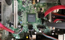
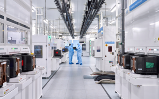
Global Foundries has been outlining the challenges in future silicon design
Global Foundries has been detailing how it will overcome the technical challenges of mass producing silicon hardware at 28nm and beyond.
Gregg Bartlett, senior vice president of process technology and R&D at Global Foundries, said at the Semicon West 2010 event in San Francisco that the company is already set for volume production of 28nm chips, and predicts that size will be the next battleground in chip rollouts.
However, there are significant technical challenges in designing smaller processors that must be overcome first.
Bartlett outlined three main areas of research that are key to the future of silicon design: materials, package integration and lithography.
The use of technologies like high k metal gates has dramatically extended the life of existing materials, he explained.
"There's no doubt that the introduction of high k metal gate is among the most revolutionary changes that the industry has gone through," said Bartlett. "In fact, it's one of the most revolutionary changes in the modern era."
Using this technology in 28nm silicon allows manufacturers to increase density by 100 per cent, with a 50 per cent cut in energy use and the same increase in speed. This could be achieved with a 10 to 20 per cent smaller die.
The main improvement in packaging technology has been in 3D stacking. Merging memory and the processor on a single die gives significant improvements in system performance, and Global Foundries will share its lead-free silicon technology with the rest of the industry.
The company's Dresden FAB has already perfected the running of high volumes of lead-free chips, according to Bartlett.
The final piece of the jigsaw, and possibly the biggest obstacle to future chip design, is lithography, the etching of designs onto substrate.
Bartlett said that Global Foundries is committed to extreme ultraviolet (EUV) lithography, which should prove effective at etching down to around 13nm to 15nm.
Global Foundries is currently using immersion lithography for chip etching, but this is running into problems, and significant hurdles must be overcome for mass production.
The company will install its first EUV units in its New York Malta plant in 2012, Bartlett said, and will then take the unusual step of skipping pre-production testing and going straight for volume production by 2014/2015.
The technological challenges facing the industry are severe, he warned, and require a collaborative approach to research, development and production, echoing similar calls from IBM.
The billions needed to develop next-generation chip architecture could only come from conglomerations of knowledge and resources, said Bartlett.